2.6 KiB
2.6 KiB
+++ math = false highlight = true tags = [] title = "ST Link v2 clone as a dev board" summary = "Notes on using an Aluminium case ST Link v2 clone as a development board" date = 2018-01-01T15:12:38+01:00 draft = false
+++ Notes on using an Aluminium case ST Link v2 clone as a development board. In summary, it can:
- Talk to the host over USB
- Blink the built-in LED (!)
- Drive a RGB LED via PWM
- Drive a 40 RGB LED pHAT over SPI
- Drive a 320x240 LCD over fast bitbanged SPI
Docs
Programming
I used a Segger J-Link to load the pre-built
STM32duino bootloader.
As the LED is on PA9, use the generic_boot20_pa9.bin version.
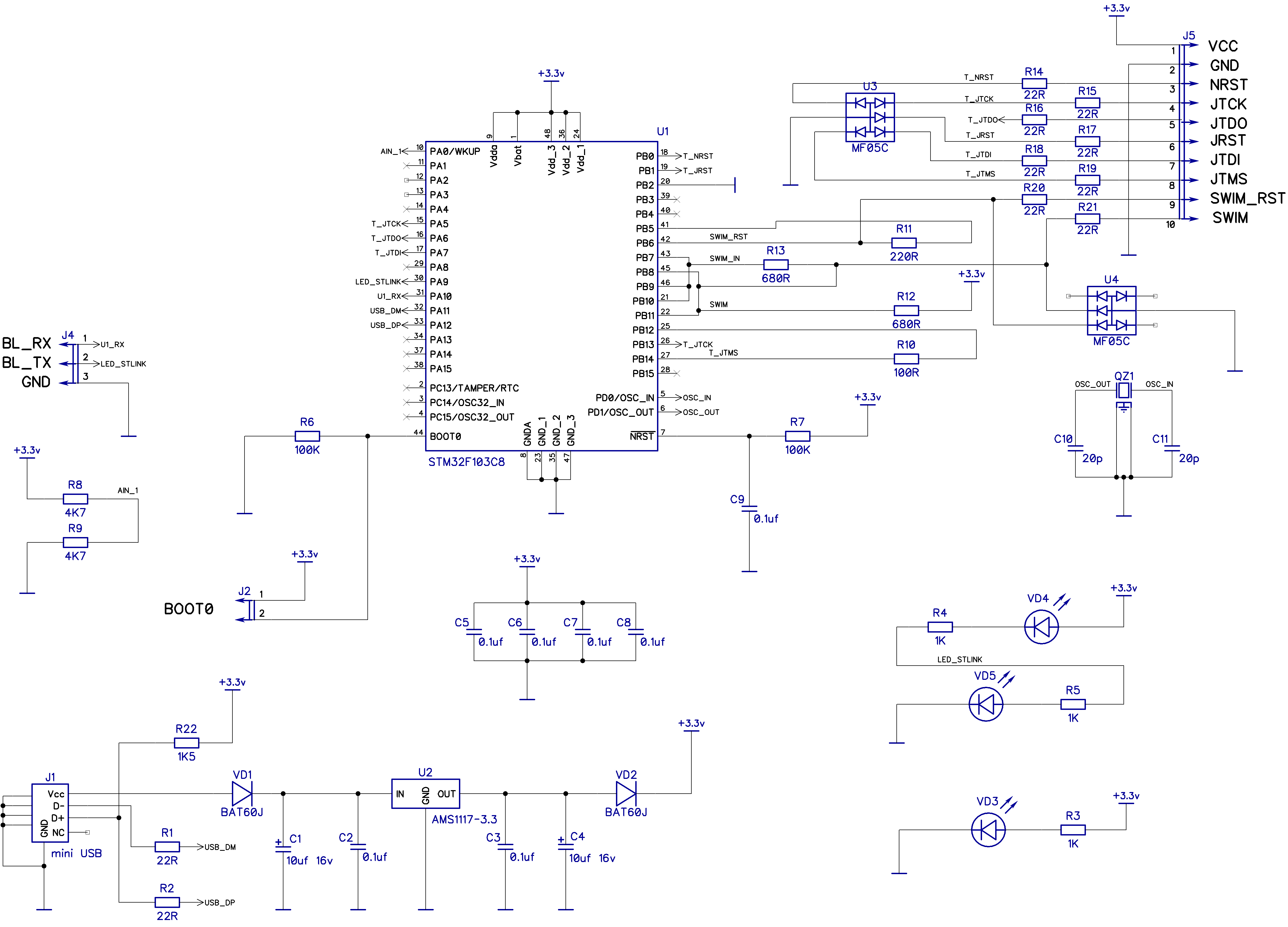
Pins
| Function | Pin | Feedback pin |
|---|---|---|
| RST | PB6 | PB5 |
| SWDIO | PB14 | PB12 |
| SWCLK | PA5 + PB13 | None |
| SWIM | PB8 + PB11 | PB7 + PB9 + PB10 |
| LED | PA9 | N/A |
The 'feedback' pins have an extra 100 R to 680 R resistor between the main pin and the feedback pin. I assume this is used to detect if the DUT is driving the pin at the same time as the debugger.
Functions
| Port | Default alternate | Remap alternate |
|---|---|---|
| PA5 | SPI1_SCK, ADC12_IN5 | None |
| PA9 (LED) | USART1_TX, TIM1_CH2 | None |
| PB5 | I2C1_SMBAI | TIM3_CH2, SPI1_MOSI |
| PB6 | I2C1_SCL, TIM4_CH1 | USART1_TX |
| PB8 | TIM4_CH3 | I2C1_SCL, CANRX |
| PB7 | I2C1_SDA, TIM4_CH2 | USART1_RX |
| PB9 | TIM4_CH4 | I2C1_SDA, CANTX |
| PB10 | I2C2_SCL, USART3_TX | TIM2_CH3 |
| PB11 | I2C2_SDA, USART3_RX | TIM2_CH4 |
| PB12 | SPI2_NSS, I2C2_SMBAI, USART3_CK, TIM1_BKIN | None |
| PB13 | SPI2_SCK, USART3_CTS, TIM1_CH1N | None |
| PB14 | SPI2_MISO, USART3_RTS, TIM1_CH2N | None |
Or, transposed:
| Function | Available features | But... |
|---|---|---|
| I2C1 | SCL, SCL, SDA | SDA is behind a 680R (might be OK) |
| I2C2 | SDA, SMBAI, SDA | No SCK |
| SPI1 | SCK, MOSI | MOSI is on a remap, and remap is all or nothing |
| SPI2 | SCK, MISO, NSS | |
| USART1 | TX, RX | Usable |
| USART3 | RX, CTS, RTS, CK, TX | TX and RX are on the same pin |